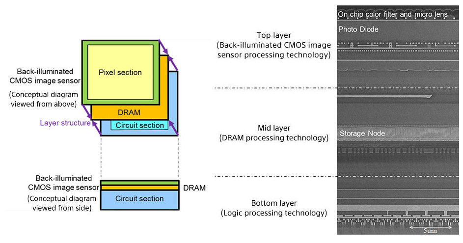
Sony today announced industry’s first 3-layer stacked CMOS image sensor with DRAM for smartphones. This has a DRAM layer added to the conventional 2-layer stacked CMOS image sensor with a layer of back-illuminated structure pixels and a chip affixed with mounted circuits for signal processing.
This promises fast data readout speeds, making it possible to capture still images of fast-moving subjects with minimal focal plane distortion as well as super slow motion movies at up to 1,000 frames per second in full HD (1920×1080 pixels) on smartphones, which lack a mechanical shutter for controlling exposure time.
In order to realize the high-speed readout, the circuit used to convert the analog video signal from pixels to a digital signal has been doubled from a 2-tier construction to a 4-tier construction in order to improve processing ability.
The sensor includes solutions for the various technical problems inherent in the design such as reduction of the noise generated between the circuits on each of the three layers.
Sony 3-layer stacked configuration with DRAM Specifications
- Effective pixel count – 5520 (H) x 3840 (V) 21.2 megapixels
- Image size (Diagonal) – 7.73mm (Type 1/2.3)
- Unit cell size – 1.22μm (H) x 1.22μm (V)
- Frame rate Still images – 30fps 4:3 19.3 megapixels / 16:9 17.1 megapixels
- Movies – 4K (3840 x 2160) at 60fps, Full HD / 720p at 240fps
- Reading speed – 8.478 ms (4:3 19.3 megapixels) / 6.962 ms (16:9 17.1 megapixels)
- Power supply 2.5V / 1.8V / 1.1V
- Image format – Bayer RAW
- Output – MIPI (CSI2) D-PHY 2.2Gbps/lane / C-PHY 2.0Gsps/lane
- DRAM capacity – 1G bit
